Samsung galaxy pcb board components 4g motherboard ic layout bluetooth solution broadcom back ripon cht wi fi How to replace 🔧🔌📱 charging port samsung galaxy note 2 gt-n7100 Schematic samsung n7100 full
GT-N7100 Galaxy Note 2 pcb Schematic - YouTube
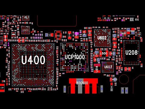
Gt-n7100 galaxy note 2 pcb schematic Ripon cht: samsung galaxy s 4g Schematic gt i9300 s4 pcb galaxy s5 samsung i9500
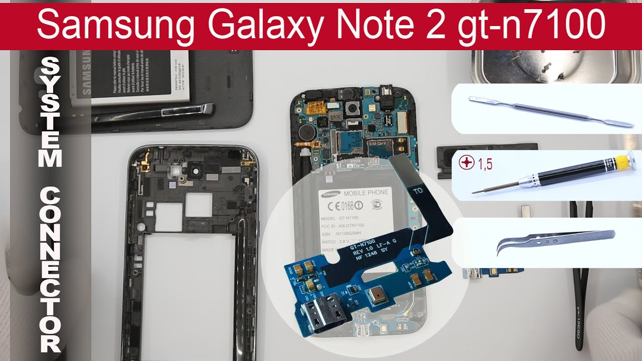
N7100 charging
.
.

Ripon Cht: Samsung Galaxy S 4G
GT-N7100 Galaxy Note 2 pcb Schematic - YouTube
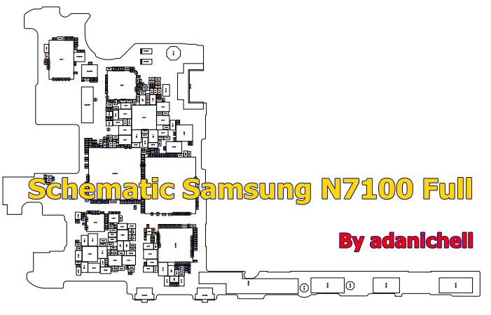
Schematic Samsung N7100 Full - AdaniChell || Tool Android
